您好,欢迎访问迅维职业技能培训学校

400-663-1699

全国咨询热线

同行寄过来板子维修实例,联想B450 LA14

机型和板号:联想B450集显,LA14

故障:南北桥!!搞了一上午

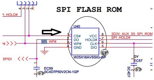
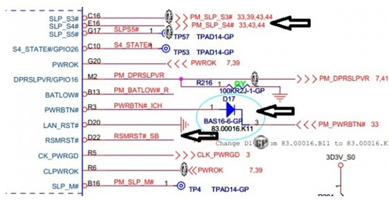
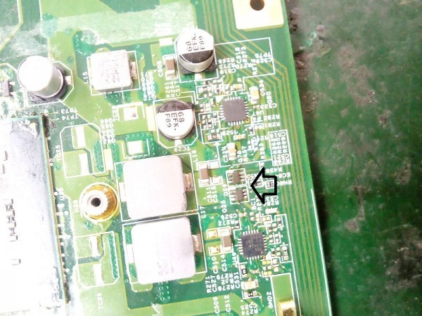
板子同行寄过的板子,拆开拿到手目测北桥有动过CPU芯片3/5待机芯片都有焊膏的痕迹,一边清洗一边观察主板各个地方看有没有其他问题,简单的目测后无发现,公共点和各大电感打值也无发现明显问题,同行也无说明故障现象,无法得知初始故障是什么。进入正式维修,接可调电源待机电流0.01(我用的稳压电源3位的,0.00几的电流会显示成0.01,这个主要为后面的故障做说明)按开关无任何反映。

SPI FLASH ROM
首先主板处于待机状态下最主要的测试点是BIOS是否有数据交换,示波器测BIOS的一脚有波形,说明EC已经读取BIOS程序定义GPIO脚位,
BIOS程序定义GPIO脚位
接下来测EC是否发出PWRBTN#给南桥,实测EC以发出PWRBTN#已经有高低高的跳变,测SLP_S5#无电压,南桥要发出SLP信号需要3/5V待机,RTC电路正常,RSMRST。测南桥的RSMRST#为低电平,测南桥的3/5V都木有。
RSMRST
待机芯片为TPS51125,PWM的3/5V开启信号为通过一个电阻接地,无法测到电压,这个有点麻烦,测Q25和Q26的2脚均有高电平,说明EC已经发出3/5V南桥待机开启信号,示波器测L15和L6,发现L6后端电压有瞬间起来就掉,测3V的上管G极无任何波形,怀疑芯片不良,更换后故障依旧,使用替换法,3/5V场馆互换,故障现象还是一样,Q25和Q26互换后发现问题了,3V出来,5V出不来,
料板
判定Q25损坏,管子找的麻烦,我把损坏的场馆拆掉,3脚和3脚互联,没想到2个都不出了,还是料板找一个了,装上去后电流直接到0.2几…


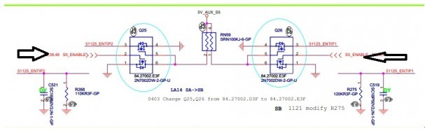
点评:
3脚和3脚连一起是不行的。因为TPS51125的ENTRIP1 和ENTRIP2不能连一起。他们的作用解释:
Channel 1 and Channel 2 enable and OCL trip setting pins.
Connect resistor from this pin to GND to set threshold for synchronous R DS(on) sense. Short to ground
to shutdown a switcher channel.
通道1和通道2开启和过流保护限定值设定脚。
通过一个电阻连接这些引脚到地,用于设定下管完全导通后检测电流的阀值。接地时,关闭两路输出。
所以说,这个2个脚是用于设定过流阀值的,连一起的话,改变了接地电阻的阻值。

附:关于过流保护的详细解释如下:
Current Protection
TPS51125 has cycle-by-cycle over current limiting control. The inductor current is monitored during the ‘ OFF ’
state and the controller keeps the ‘ OFF ’ state during the inductor current is larger than the over current trip level.
In order to provide both good accuracy and cost effective solution, TPS51125 supports temperature
compensated MOSFET R DS(on) sensing. ENTRIPx pin should be connected to GND through the trip voltage
setting resistor, R TRIP . ENTRIPx terminal sources I TRIP current, which is 10 µ A typically at room temperature, and
the trip level is set to the OCL trip voltage V TRIP as below. Note that the V TRIP is limited up to about 205 mV
internally.

The inductor current is monitored by the voltage between GND pin and LLx pin so that LLx pin should be
connected to the drain terminal of the bottom MOSFET properly. Itrip has 4500 ppm/ ° C temperature slope to
compensate the temperature dependency of the R DS(on) . GND is used as the positive current sensing node so
that GND should be connected to the proper current sensing device, i.e. the source terminal of the bottom
MOSFET.
As the comparison is done during the ‘ OFF ’ state, V TRIP sets valley level of the inductor current. Thus, the load
current at over current threshold, I OCP , can be calculated as follows;


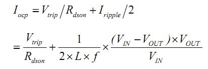
In an over current condition, the current to the load exceeds the current to the output capacitor thus the output
voltage tends to fall down. Eventually, it ends up with crossing the under voltage protection threshold and
shutdown both channels.


学到熟练维修 需要多少钱?
当前水平
零基础
会拆装
会修小问题
计划学习时间
1~2个月全天上课
利用闲暇时间学习

 联系方式

培训咨询点击这里给我发消息

技术交流群迅维网官方群7

加微信,和老师沟通
一下技术问题!
扫一扫添加客服老师
联系我们

加微信,和老师沟通一下技术问题!

打开微信,点击右上角的“+”,

选择“扫一扫”功能,

用摄像头对准下方二维码即可。


客服老师

恭喜你,获得维修课程一节

添加老师微信,帮你一对一安排试听课

了解试听需求

安排试听时间

微信号:13691708525

复制微信号添加